I was assigned on a failure analysis project for one of my companies top customers. This project’s overview was that a specific SFP transceiver vendor was not detectable by software. The system overview is that the CPU will communicate with the SFP via the I²C bus through multiple I²C switch chips.
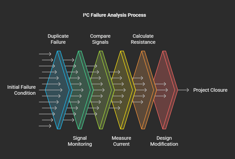
The failure analysis process was as follows:
- Duplicate the failure condition and ensure the failure is repeatable. This will expeditie debugging.
- Use a four channel oscilloscope to monitor multiple stages of the I²C bus for signal integrity. Since the design has multiple stages of I²C switches, each channel was placed strategically – one placed near the CPU, two placed between switches and one placed at the SFP.
- Compare the signals between a known working and verified SFP with the failing SFP and found that the failing SFP SDA line was not pulling down from 3.3V to 0V.
- Measure the SDA current at the SFP port and it measured over the I²C standard of 3mA.
- Do a calculation of the pull up resistors in parallel and found there were too many pull up resistors in parallel which reduced the equivalent resistance, thus the high current value. The SFP was unable to sink the high current.
- Bring the FA to our internaltional team based in Taiwan who is responsible for design changes and present the results and to reduce the number of resistors in parallel to increase the equivalent resistance and bring the current back in spec.
- Follow the change process through Oracle Agile for accurate ECOs, rework instructions and test reports.
- Ensure all changes have been approved and the solution implemented in the factory and close the project.

Leave a comment